As the digital world hurries towards an era dominated by artificial intelligence, high-performance computing (HPC), and pervasive connectivity, the foundational material of modern electronics—silicon—is rapidly approaching its physical limits. A quiet but profound revolution is underway in material science and semiconductor manufacturing, with recent innovations in novel materials and advanced fabrication techniques promising to unlock unprecedented levels of chip performance, energy efficiency, and manufacturing agility. This shift, particularly prominent from late 2024 through 2025, is not merely an incremental upgrade but a fundamental re-imagining of how microchips are built, with far-reaching implications for every sector of technology.
The immediate significance of these advancements cannot be overstated. From powering more intelligent AI models and enabling faster 5G/6G communication to extending the range of electric vehicles and enhancing industrial automation, these next-generation semiconductors are the bedrock upon which future technological breakthroughs will be built. The industry is witnessing a concerted global effort to invest in research, development, and new manufacturing plants, signaling a collective understanding that the future of computing lies "beyond silicon."
The Science of Speed and Efficiency: A Deep Dive into Next-Gen Materials
The core of this revolution lies in the adoption of materials with superior intrinsic properties compared to silicon. Wide-bandgap semiconductors, two-dimensional (2D) materials, and a host of other exotic compounds are now moving from laboratories to production lines, fundamentally altering chip design and capabilities.
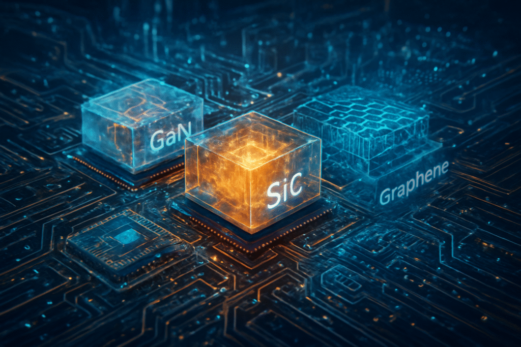
Wide-Bandgap Semiconductors: GaN and SiC Lead the Charge
Gallium Nitride (GaN) and Silicon Carbide (SiC) are at the forefront of this material paradigm shift, particularly for high-power, high-frequency, and high-voltage applications. GaN, with its superior electron mobility, enables significantly faster switching speeds and higher power density. This makes GaN ideal for RF communication, 5G infrastructure, high-speed processors, and compact, efficient power solutions like fast chargers and electric vehicle (EV) components. GaN chips can operate up to 10 times faster than traditional silicon and contribute to a 10 times smaller CO2 footprint in manufacturing. In data center applications, GaN-based chips achieve 97-99% energy efficiency, a substantial leap from the approximately 90% for traditional silicon. Companies like Infineon Technologies AG (ETR: IFX), Taiwan Semiconductor Manufacturing Company (TSMC) (NYSE: TSM), and Navitas Semiconductor Corporation (NASDAQ: NVTS) are aggressively scaling up GaN production.
SiC, on the other hand, is transforming power semiconductor design for high-voltage applications. It can operate at higher voltages and temperatures (above 200°C and over 1.2 kV) than silicon, with lower switching losses. This makes SiC indispensable for EVs, industrial automation, and renewable energy systems, leading to higher efficiency, reduced heat waste, and extended battery life. Wolfspeed, Inc. (NYSE: WOLF), a leader in SiC technology, is actively expanding its global production capacity to meet burgeoning demand.
Two-Dimensional Materials: Graphene and TMDs for Miniaturization
For pushing the boundaries of miniaturization and introducing novel functionalities, two-dimensional (2D) materials are gaining traction. Graphene, a single layer of carbon atoms, boasts exceptional electrical and thermal conductivity. Electrons move more quickly in graphene than in silicon, making it an excellent conductor for high-speed applications. A significant breakthrough in 2024 involved researchers successfully growing epitaxial semiconductor graphene monolayers on silicon carbide wafers, opening the energy bandgap of graphene—a long-standing challenge for its use as a semiconductor. Graphene photonics, for instance, can enable 1,000 times faster data transmission. Transition Metal Dichalcogenides (TMDs), such as Molybdenum Disulfide (MoS₂), naturally possess a bandgap, making them directly suitable for ultra-thin transistors, sensors, and flexible electronics, offering excellent energy efficiency in low-power devices.
Emerging Materials and Manufacturing Innovations
Beyond these, materials like Carbon Nanotubes (CNTs) promise smaller, faster, and more energy-efficient transistors. Researchers at MIT have identified cubic boron arsenide as a material that may outperform silicon in both heat and electricity conduction, potentially addressing two major limitations, though its commercial viability is still nascent. New indium-based materials are being developed for extreme ultraviolet (EUV) patterning in lithography, enabling smaller, more precise features and potentially 3D circuits. Even the accidental discovery of a superatomic material (Re₆Se₈Cl₂) by Columbia University researchers, which exhibits electron movement potentially up to a million times faster than in silicon, hints at the vast untapped potential in material science.
Crucially, glass substrates are revolutionizing chip packaging by allowing for higher interconnect density and the integration of more chiplets into a single package, facilitating larger, more complex assemblies for data-intensive applications. Manufacturing processes themselves are evolving with advanced lithography (EUV with new photoresists), advanced packaging (chiplets, 2.5D, and 3D stacking), and the increasing integration of AI and machine learning for automation, optimization, and defect detection, accelerating the design and production of complex chips.
Competitive Implications and Market Shifts in the AI Era
These material science breakthroughs and manufacturing innovations are creating significant competitive advantages and reshaping the landscape for AI companies, tech giants, and startups alike.
Companies deeply invested in high-power and high-frequency applications, such as those in the automotive (EVs), renewable energy, and 5G/6G infrastructure sectors, stand to benefit immensely from GaN and SiC. Automakers adopting SiC in their power electronics will see improved EV range and charging times, while telecommunications companies deploying GaN can build more efficient and powerful base stations. Power semiconductor manufacturers like Wolfspeed and Infineon, with their established expertise and expanding production, are poised to capture significant market share in these growing segments.
For AI and HPC, the push for faster, more energy-efficient processors makes materials like graphene, TMDs, and advanced packaging solutions critical. Tech giants like NVIDIA Corporation (NASDAQ: NVDA), Intel Corporation (NASDAQ: INTC), and Advanced Micro Devices, Inc. (NASDAQ: AMD), who are at the forefront of AI accelerator development, will leverage these innovations to deliver more powerful and sustainable computing platforms. The ability to integrate diverse chiplets (CPUs, GPUs, AI accelerators) using advanced packaging techniques, spearheaded by TSMC (NYSE: TSM) with its CoWoS (Chip-on-Wafer-on-Substrate) technology, allows for custom, high-performance solutions tailored for specific AI workloads. This heterogeneous integration reduces reliance on monolithic chip designs, offering flexibility and performance gains previously unattainable.
Startups focused on novel material synthesis, advanced packaging design, or specialized AI-driven manufacturing tools are also finding fertile ground. These smaller players can innovate rapidly, potentially offering niche solutions that complement the larger industry players or even disrupt established supply chains. The "materials race" is now seen as the new Moore's Law, shifting the focus from purely lithographic scaling to breakthroughs in materials science, which could elevate companies with strong R&D in this area. Furthermore, the emphasis on energy efficiency driven by these new materials directly addresses the growing power consumption concerns of large-scale AI models and data centers, offering a strategic advantage to companies that can deliver sustainable computing solutions.
A Broader Perspective: Impact and Future Trajectories
These semiconductor material innovations fit seamlessly into the broader AI landscape, acting as a crucial enabler for the next generation of intelligent systems. The insatiable demand for computational power to train and run ever-larger AI models, coupled with the need for efficient edge AI devices, makes these material advancements not just desirable but essential. They are the physical foundation for achieving greater AI capabilities, from real-time data processing in autonomous vehicles to more sophisticated natural language understanding and generative AI.
The impacts are profound: faster inference speeds, reduced latency, and significantly lower energy consumption for AI workloads. This translates to more responsive AI applications, lower operational costs for data centers, and the proliferation of AI into power-constrained environments like wearables and IoT devices. Potential concerns, however, include the complexity and cost of manufacturing these new materials, the scalability of some emerging compounds, and the environmental footprint of new chemical processes. Supply chain resilience also remains a critical geopolitical consideration, especially with the global push for localized fab development.
These advancements draw comparisons to previous AI milestones where hardware breakthroughs significantly accelerated progress. Just as specialized GPUs revolutionized deep learning, these new materials are poised to provide the next quantum leap in processing power and efficiency, moving beyond the traditional silicon-centric bottlenecks. They are not merely incremental improvements but fundamental shifts that redefine what's possible in chip design and, consequently, in AI.
The Horizon: Anticipated Developments and Expert Predictions
Looking ahead, the trajectory of semiconductor material innovation is set for rapid acceleration. In the near-term, expect to see wider adoption of GaN and SiC across various industries, with increased production capacities coming online through late 2025 and into 2026. TSMC (NYSE: TSM), for instance, plans to begin volume production of its 2nm process in late 2025, heavily relying on advanced materials and lithography. We will also witness a significant expansion in advanced packaging solutions, with chiplet architectures becoming standard for high-performance processors, further blurring the lines between different chip types and enabling unprecedented integration.
Long-term developments will likely involve the commercialization of more exotic materials like graphene, TMDs, and potentially even cubic boron arsenide, as manufacturing challenges are overcome. The development of AI-designed materials for HPC is also an emerging market, promising improvements in thermal management, interconnect density, and mechanical reliability in advanced packaging solutions. Potential applications include truly flexible electronics, self-powering sensors, and quantum computing materials that can improve qubit coherence and error correction.
Challenges that need to be addressed include the cost-effective scaling of these novel materials, the development of robust and reliable manufacturing processes, and the establishment of resilient supply chains. Experts predict a continued "materials race," where breakthroughs in material science will be as critical as advancements in lithography for future progress. The convergence of material science, advanced packaging, and AI-driven design will define the next decade of semiconductor innovation, enabling capabilities that are currently only theoretical.
A New Era of Computing: The Unfolding Story
In summary, the ongoing revolution in semiconductor materials represents a pivotal moment in the history of computing. The move beyond silicon to wide-bandgap semiconductors like GaN and SiC, coupled with the exploration of 2D materials and other exotic compounds, is fundamentally enhancing chip performance, energy efficiency, and manufacturing flexibility. These advancements are not just technical feats; they are the essential enablers for the next wave of artificial intelligence, high-performance computing, and ubiquitous connectivity, promising a future where computing power is faster, more efficient, and seamlessly integrated into every aspect of life.
The significance of this development in AI history cannot be overstated; it provides the physical muscle for the intelligent algorithms that are transforming our world. As global investments pour into new fabs, particularly in the U.S., Japan, Europe, and India, and material science R&D intensifies, the coming months and years will reveal the full extent of this transformation. Watch for continued announcements regarding new material commercialization, further advancements in advanced packaging technologies, and the increasing integration of AI into the very process of chip design and manufacturing. The materials race is on, and its outcome will shape the digital future.
This content is intended for informational purposes only and represents analysis of current AI developments.
TokenRing AI delivers enterprise-grade solutions for multi-agent AI workflow orchestration, AI-powered development tools, and seamless remote collaboration platforms.
For more information, visit https://www.tokenring.ai/.